Όλες οι κατηγορίες
-
Ολοκληρωμένα κυκλώματα (ICs)
Ολοκληρωμένα κυκλώματα (ICs)
- Διασύνδεση - αισθητήρας, χωρητική επαφή(642)
- Εξειδικευμένες ICs(12302)
- Το POLMIC - ρυθμιστές τάσης - ειδικού σκοπού(5644)
- Ρυθμιστές τάσης PMIC - Ελεγκτές γραμμικού ρυθμιστή(793)
- PMIC - Ρυθμιστές τάσης - Γραμμική + εναλλαγή(1829)
- Το POLMIC - ρυθμιστές τάσης - γραμμική(70981)
- Ρυθμιστές τάσης PMIC - Ρυθμιστές μεταγωγής DC DC(39569)
- Ρυθμιστές τάσης PMIC - Ελεγκτές μεταγωγής DC DC DC(13507)
- Το POLMIC - τάσης αναφοράς(9453)
- Το POLMIC - V/F και των Φ/Β μετατροπέων(145)
- Το POLMIC - θερμική διαχείριση(592)
- Το POLMIC - επόπτες(47946)
- Το POLMIC - RMS DC μετατροπείς(170)
- Το POLMIC - Power εφοδιασμού ελεγκτές, οθόνες(2104)
- Το POLMIC - Power Over Ethernet (PoE) ελεγκτές(1008)
- Το POLMIC - διαχείριση ενέργειας - εξειδικευμένες(7722)
- Drivers Load PMIC - διακόπτες διανομής ισχύος,(7706)
- Το POLMIC - PFC (διόρθωση συντελεστή ισχύος)(1222)
- Το POLMIC - ή ελεγκτές, ιδανικό δίοδοι(705)
- Ελεγκτές PMIC - προγράμματα οδήγησης με κινητήρα,(4712)
- Το POLMIC - φωτισμός, έρμα ελεγκτές(560)
- Το POLMIC - οδήγησε οδήγησης(7282)
- Το POLMIC - λέιζερ οδηγοί(573)
- Το POLMIC - Hot Swap ελεγκτές(2816)
- Το POLMIC - οδηγούς πύλη(7083)
- Το POLMIC - πλήρη και μισή γέφυρα οδήγησης(1342)
- Το POLMIC - ενεργειακή μέτρηση(654)
- Το POLMIC - προγράμματα οδήγησης οθόνης(1435)
- Το POLMIC - τρέχουσα ρύθμιση/διαχείριση(1481)
- Το POLMIC - διαχείριση μπαταρίας(5553)
- Το POLMIC - φορτιστές μπαταριών(3831)
- Μετατροπείς PMIC - AC DC, διακόπτες εκτός σύνδεσης(4905)
- Μνήμη - ελεγκτές(358)
- Μνήμη - διαμόρφωση Proms για FPGAs(639)
- Μνήμης - μπαταρίες(13)
- Μνήμη(65694)
- Λογική - καθολική λεωφορείο λειτουργίες(706)
- Λογική - μεταφραστές, μετατοπιστές στάθμης(2854)
- Λογική - ειδικότητα λογική(1870)
- Λογική - διακόπτες σήματος, πολυπλέκτες, αποκωδικοποιητές(9420)
- Λογική - καταγραφείς μετατόπισης(2665)
- Λογική - ισοτιμία γεννήτριες και πούλια(335)
- Λογική - Multivibrators(831)
- Λογική - σύρτες(3658)
- Λογική - πύλες και μετατροπείς - Πολλαπλές λειτουργίες, διαμορφώσιμες(1687)
- Λογική - πύλες και μετατροπείς(16453)
- Λογική - σαγιονάρες(7780)
- Λογική - FIFOs μνήμη(4240)
- Λογική - μετρητές, διαχωριστικά(3456)
- Λογική - συγκριτές(592)
- Λογική - buffer, οδηγοί, δέκτες, πομποδέκτες(17835)
- Γραμμικά - επεξεργασία βίντεο(2909)
- Γραμμική - συγκριτές(5084)
- Γραμμικός - αναλογικοί πολλαπλασιαστές, διαχωριστές(263)
- Γραμμική - βίντεο ενισχυτές και ενότητες(1905)
- Γραμμική - ενισχυτές - ειδικού σκοπού(1856)
- Γραμμικοί - ενισχυτές - όργανα, ενισχυτές op, ενισχυτές buffer(34236)
- Γραμμική - ενισχυτές - ήχου(4567)
- Διεπαφή - φωνητική εγγραφή και αναπαραγωγή(556)
- Διασύνδεση - UARTS (Universal ασύγχρονος πομπός δέκτη)(1237)
- Διεπαφή - Telecom(4467)
- Διεπαφή - εξειδικευμένες(4833)
- Διεπαφή - εξολοθρευτές του σήματος(333)
- Διεπαφή - buffers σήματος, επαναλήπτες, διαχωριστές(1449)
- Διεπαφή - Serializers, Deserializers(1480)
- Διεπαφή - αισθητήρα και ανιχνευτή διασυνδέσεις(1524)
- Διεπαφή - ενότητες(169)
- Διεπαφή - Modems - ICs και ενότητες(407)
- Διεπαφή - επέκτασης εισόδου/εξόδου(1136)
- Διεπαφή - φίλτρα - ενεργού(1226)
- Διασύνδεση - κωδικοποιητές, αποκωδικοποιητές, μετατροπείς(714)
- Διεπαφή - οδηγούς, δέκτες, πομποδέκτες(20755)
- Διεπαφή - άμεση ψηφιακή σύνθεση (DDS)(117)
- Διεπαφή - ελεγκτές(3628)
- Διεπαφή - κωδικοποιητές(1676)
- Διεπαφή - Αναλογικοί διακόπτες, πολυπλέκτες, αποπολιπλόνες(12567)
- Διεπαφή - αναλογικών διακοπτών - ειδικού σκοπού(2533)
- Το ενσωματωμένο - σύστημα σε τσιπ (SoC)(4496)
- Ενσωματωμένα - PLDs (προγραμματιζόμενη λογική συσκευή)(971)
- Ενσωματωμένο - μικροεπεξεργαστές(10083)
- Ενσωματωμένα - Μικροελεγκτές - Ειδικά για εφαρμογή(2275)
- Ενσωματωμένο - μικροελεγκτές(99285)
- Ενσωματωμένο - μικροελεγκτή, μικροεπεξεργαστή, μονάδες FPGA(1527)
- Ενσωματωμένο - FPGAs (Προγραμματιζόμενη συστοιχία πύλης πεδίου) με μικροελεγκτές(81)
- Ενσωματωμένο - FPGAS (Προγραμματιζόμενη συστοιχία πύλης πεδίου)(27747)
- Ενσωματωμένο - DSP (ψηφιακοί επεξεργαστές σήματος)(4081)
- Ενσωματωμένο - CPLDs (σύνθετες προγραμματιζόμενες λογικές συσκευές)(5187)
- Απόκτηση δεδομένων - χειριστήρια οθόνης αφής(1210)
- Απόκτηση δεδομένων - Μετατροπείς ψηφιακών σε αναλογικούς (DAC)(14419)
- Απόκτηση δεδομένων - ψηφιακά ποτενσιόμετρα(6250)
- Απόκτηση δεδομένων - Αναλογικοί σε ψηφιακούς μετατροπείς (ADC)(17776)
- Απόκτηση δεδομένων - Αναλογικό μπροστινό μέρος (AFE)(787)
- Δεδομένα - ADCs/DACs - απόκτηση ειδικού σκοπού(3043)
- Ρολόι/χρονισμός - ρολόγια σε πραγματικό χρόνο(2446)
- Ρολόι/χρονισμός - προγραμματιζόμενοι χρονομετρητές και ταλαντωτές(23469)
- Ρολόι/χρονοδιάγραμμα - IC μπαταρίες(4)
- Ρολόι/χρονοδιάγραμμα - καθυστέρηση γραμμές(1049)
- Ρολόι/χρονισμός - Γεννήτριες ρολογιού, PLLs, συνθέτες συχνότητας(32775)
- Ρολόι/χρονισμός - buffers ρολογιού, οδηγοί(4568)
- Ρολόι/χρονοδιάγραμμα - ειδικών εφαρμογών(8652)
- Ήχου ειδικού σκοπού(1564)
Σχετικός κατασκευαστής


-
Προϊόντα διακριτών ημιαγωγών
Προϊόντα διακριτών ημιαγωγών
- Τρέχουσα ρύθμιση - Δίοδοι, τρανζίστορ(1090)
- Τρανζίστορ - Ειδικός σκοπός(226)
- Τρανζίστορ - προγραμματιζόμενη μία Ένωση(48)
- Τρανζίστορ - JFETs(1558)
- ΤΡΑΝΖΙΣΤΟΡΣ - IGBTs - Single(4799)
- ΤΡΑΝΖΙΣΤΟΡΣ - IGBTs - ενότητες(63420)
- ΤΡΑΝΖΙΣΤΟΡΣ - IGBTs - πίνακες(26)
- Τρανζίστορ - τρανζίστορ, MOSFETs - Single(48330)
- Τρανζίστορ - τρανζίστορ, MOSFETs - RF(4903)
- Τρανζίστορ - τρανζίστορ, MOSFETs - πίνακες(6641)
- Τρανζίστορ - διπολικό (BJT) - Ενιαίο, προ -προκατειλημμένο(4539)
- Τρανζίστορ - διπολική (BJT) - ενιαία(25800)
- ΤΡΑΝΖΙΣΤΟΡΣ - διπολική (BJT) - RF(2087)
- Τρανζίστορ - διπολικά (BJT) - συστοιχίες, προ -προκατειλημμένα(2115)
- ΤΡΑΝΖΙΣΤΟΡΣ - διπολική (BJT) - πίνακες(2310)
- Θυρίστορ - θυρίστορ αμφίδρομης διέλευσης(4044)
- Θυρίστορ - SCRs - ενότητες(3967)
- Θυρίστορ - SCRs(5436)
- Θυρίστορ - διάκ, SIDACs(319)
- Μονάδες οδήγησης ισχύος(1627)
- Δίοδοι - Zener - Single(87483)
- Δίοδοι - Zener - πίνακες(2619)
- Δίοδοι - Μεταβλητή χωρητικότητα (Varicaps, Varactors)(1200)
- Δίοδοι - RF(2753)
- Δίοδοι - ΑΝΟΡΘΩΤΕΣ - Single(67528)
- Δίοδοι - ανορθωτές - συστοιχίες(20581)
- Δίοδοι - Γέφυρες ανόρθωσης(11700)
Σχετικός κατασκευαστής


-
RF / IF και RFID
RF / IF και RFID
- Κάρτες αναγνώρισης συνδρομητή (SIM)(77)
- RF κυκλοφορητές και απομονωτές(1742)
- RFID, RF πρόσβαση, παρακολούθηση ICs(1550)
- Αναμεταδότες RFID, Ετικέτες(747)
- Λειτουργικές μονάδες ανάγνωσης RFID(464)
- RFID Αξιολόγηση και Ανάπτυξη κιτ, πίνακες(30)
- Κεραιών RFID(329)
- RFI και ΕΝΙ - θωράκιση και απορροφώντας υλικών(6444)
- RFI και EMI - Επαφές, δάχτυλα και παρεμβύσματα(7497)
- Πομποί RF(668)
- Πομποδεκτης RF ενότητες(6900)
- Πομποδεκτης RF ICs(4169)
- RF διακόπτες(9276)
- RF ασπίδες(16401)
- RF δέκτες(1998)
- RF δέκτης και πομπός πομποδέκτη τελειώσει μονάδες(2763)
- Διαχωριστικά τροφοδοσίας RF/θραύστες(1223)
- Τροφοδοσίας RF ελεγκτή ICs(86)
- Διαμορφωτές RF(710)
- RF μίξερ(2800)
- RF Misc ICs και ενότητες(3276)
- RF Front End (LNA + PA)(419)
- RF αξιολόγηση και κιτ ανάπτυξης, πίνακες(747)
- RF κατευθυντικός συζεύκτης(2718)
- Διακλαδωτές RF(1464)
- Ανιχνευτές RF(412)
- RF Demodulators(249)
- Κεραίες RF(12319)
- Ενισχυτές RF(19651)
- Balun(1496)
- Εξασθενητές(4852)
Σχετικός κατασκευαστής


-
Οπτοηλεκτρονική
Οπτοηλεκτρονική
- Οπτομ -μηχανικός(480)
- Φωτιστικά(125)
- Δίοδοι λέιζερ, μονάδες λέιζερ - Παράδοση λέιζερ, ίνες λέιζερ(345)
- Συστήματα λέιζερ Hene(31)
- Κεφαλές λέιζερ Hene(27)
- Εμφάνιση οπίσθιων φωτιστικών(93)
- Φωτισμό xenon(387)
- Αφής οθόνη επικαλύψεις(453)
- Πίνακας δεικτών, πιλότος φώτα(75729)
- Οπτικά - απομακρυσμένη Φωσφόρος πηγής φωτός(269)
- Οπτικά - ανακλαστήρες(665)
- Οπτικά - Φωτοσωλήνες(5384)
- Οπτικά - φακοί(4951)
- LED - διαχωριστικά, διαχωριστικά(2718)
- LED - αντικαταστάσεις λυχνίας(29718)
- LED - Δείκτες πλακέτας κυκλώματος, συστοιχίες, ελαφριές ράβδους, γραφήματα μπαρ(9083)
- Θερμικό LED προϊόντα(667)
- Πακέτα φωτισμού LED(64)
- Φωτισμός LED - λευκό(37580)
- LED φωτισμός - χρώμα(4728)
- Φωτισμού LED - στάχυα, κινητήρες, μονάδες(28735)
- Ένδειξη LED - διακριτά(27601)
- Δίοδοι λέιζερ, Ενότητες(1553)
- Λάμπες - λαμπτήρες πυρακτώσεως, Neons(311004)
- Λάμπες - Ψυχρό κάθοδο φθορίζον (CCFL) & amp;UV(164)
- Μετατροπείς(7728)
- Υπέρυθρες, UV, ορατές ακτινοβολίες(3871)
- Οπτικά ινών - πομποί - Ενσωματωμένο κύκλωμα κίνησης(4085)
- Οπτικών ινών - πομποί - διακριτά(350)
- Οπτικών ινών - ενότητες πομποδεκτών(18758)
- Οπτικές ίνες - διακόπτες, πολυπλέκτες, αποπολιπλόνες(1387)
- Οπτικών ινών - δέκτες(695)
- Οπτικών ινών - εξασθενητές(654)
- Ηλεκτροφωταύγεια(102)
- Οθόνη, οθόνη - διασύνδεση ελεγκτή(98)
- Μονάδες προβολής - κενού φθορισμού (VFD)(249)
- Εμφάνιση μονάδων - LED DOT Matrix and Cluster(865)
- Εμφάνιση μονάδων - LED χαρακτήρα και αριθμητικό(5421)
- Εμφάνιση μονάδων - LCD, OLED, γραφικό(4654)
- Εμφάνιση μονάδων - LCD, χαρακτήρας OLED και αριθμητικοί(2202)
- Οθόνη Bezels, φακοί(88)
- Μπορούν να χρησιμοποιηθούν, ειδικότητας(458)
Σχετικός κατασκευαστής


-
Αισθητήρες, Μορφοτροπείς
Αισθητήρες, Μορφοτροπείς
- Υπερηχητικοί δέκτες, πομποί - βιομηχανικοί(115)
- Αισθητήρες θερμοκρασίας - Θερμοστάτες - Μηχανικοί - Βιομηχανικοί(3103)
- Αισθητήρες θερμοκρασίας - Αναλογική και ψηφιακή έξοδος - Βιομηχανία(209)
- Αισθητήρες εγγύτητας - βιομηχανικοί(13611)
- Αισθητήρες πίεσης, μετατροπείς - βιομηχανικοί(26503)
- Οπτικοί αισθητήρες - Φωτονική - Μετρητές, ανιχνευτές, SPCM (μονάδα μέτρησης φωτονίων)(751)
- Οπτικοί αισθητήρες - Μονάδες κάμερας(875)
- Μαγνητικοί αισθητήρες - θέση, εγγύτητα, ταχύτητα (ενότητες) - Βιομηχανία(554)
- Αισθητήρες δύναμης - Βιομηχανικοί(346)
- Αισθητήρες ροής - Βιομηχανικοί(151)
- Float, αισθητήρες επιπέδων - βιομηχανικοί(310)
- Κωδικοποιητές - βιομηχανικοί(4980)
- Αισθητήρες χρωμάτων - βιομηχανικοί(50)
- Αισθητήρες αφής(100)
- Υπερήχων δέκτες, πομπούς(2421)
- Αισθητήρες θερμοκρασίας - Θερμοστάτες - στερεά κατάσταση(1096)
- Μηχανική - Θερμοστάτες - αισθητήρες θερμοκρασίας(3397)
- Αισθητήρες θερμοκρασίας - Θερμοσιλεία, ανιχνευτές θερμοκρασίας(1921)
- Αισθητήρες θερμοκρασίας - RTD (ανιχνευτής θερμοκρασίας αντίστασης)(1525)
- Αισθητήρες θερμότητας - θερμίστορ PTC(2273)
- Αισθητήρες θερμότητας - θερμίστορ NTC(13259)
- Αισθητήρες θερμοκρασίας - Αναλογική και ψηφιακή έξοδος(3928)
- Δυναμοκυψέλες(1399)
- Αισθητήρες εξειδικευμένες(1861)
- Ηλιακά κύτταρα(503)
- Αισθητήρες κραδασμού(84)
- Διεπαφή αισθητήρα - διασταύρωση μπλοκ(2519)
- Καλώδιο του αισθητήρα - συνελεύσεις(22011)
- Αισθητήρες εγγύτητας/κατοχής - Τελειωμένες μονάδες(725)
- Αισθητήρες εγγύτητας(2860)
- Αισθητήρες πίεσης, μετατροπείς(11317)
- Θέση αισθητήρες - γωνία, γραμμική θέση μέτρησης(6022)
- Οπτικοί αισθητήρες - Ανακλαστική - Λογική έξοδος(194)
- Οπτικοί αισθητήρες - αντανακλαστική - αναλογική έξοδος (432)
- Αισθητήρες φωτοοπτικοί - Phototransistors(1027)
- Οπτικοί αισθητήρες - PhotoInterrupters - Τύπος υποδοχής - Έξοδος τρανζίστορ(1427)
- Οπτικοί αισθητήρες - PhotoInterrupters - Τύπος υποδοχής - Λογική έξοδος(1215)
- Οπτικοί αισθητήρες - φωτοηλεκτρικό, βιομηχανικό(16763)
- Αισθητήρες φωτοοπτικοί - φωτοδίοδοι(1543)
- Οπτικοί αισθητήρες - ανιχνευτές φωτογραφιών - απομακρυσμένος δέκτης(2605)
- Οπτικοί αισθητήρες - ανιχνευτές φωτογραφιών - Λογική έξοδος(146)
- Οπτικοί αισθητήρες - ανιχνευτές φωτογραφιών - κύτταρα CDS(74)
- Αισθητήρες φωτοοπτικοί - μέτρησης απόστασης(377)
- Οπτικοί αισθητήρες - Φως περιβάλλοντος, IR, αισθητήρες UV(1305)
- Πολλαπλών λειτουργιών(558)
- Αισθητήρες κίνησης - δόνησης(337)
- Ανιχνευτές κίνησης - διακόπτες κλίσης(67)
- Οπτικοί αισθητήρες κίνησης-(719)
- Αισθητήρες κίνησης - κλίσεων(175)
- Αισθητήρες κίνησης - IMUS (μονάδες αδρανειακής μέτρησης)(416)
- Αισθητήρες κίνησης - γυροσκόπια(214)
- Αισθητήρες κίνησης - επιταχυνσιόμετρα(1911)
- Μαγνήτες - αισθητήρα που ταιριάζουν(119)
- Μαγνήτες - πολλαπλών χρήσεων(1965)
- Μαγνητικοί αισθητήρες - Διακόπτες (στερεή κατάσταση)(3700)
- Μαγνητικοί αισθητήρες - θέση, εγγύτητα, ταχύτητα (ενότητες)(5199)
- Μαγνητικοί αισθητήρες - γραμμική, πυξίδα (ICs)(1247)
- Μαγνητικοί αισθητήρες - πυξίδα, μαγνητικό πεδίο (ενότητες)(35)
- Μετατροπείς LVDT (γραμμική μεταβλητή διαφορικού μετασχηματιστή)(204)
- Ενότητες πομποδέκτη IrDA(196)
- Αισθητήρες εικόνας, φωτογραφική μηχανή(2235)
- Υγρασία, αισθητήρες υγρασίας(1425)
- Αισθητήρες αερίου(1217)
- Αισθητήρες δύναμης(188)
- Αισθητήρες ροής(550)
- Float, αισθητήρες στάθμης(1343)
- Κωδικοποιητές(6357)
- Σκόνη αισθητήρες(43)
- Τρέχουσα μετατροπείς(3455)
- Αισθητήρες χρωμάτων(85)
- Ενισχυτές(1905)
Σχετικός κατασκευαστής


-
Σύνδεσμοι, διασυνδέσεις
Σύνδεσμοι, διασυνδέσεις
- Συνδέσεις USB, DVI, HDMI(446)
- Σύνδεσμοι φωτισμού στερεάς κατάστασης(555)
- Πρίζες για ICS, τρανζίστορ(953)
- Συνδετήρες pluggable(1221)
- Φωτοβολταϊκοί (ηλιακοί πίνακες) Συνδέσμοι(136)
- Συνδετήρες οπτικών ινών(370)
- Σύνδεσμοι FFC, FPC (επίπεδη ευέλικτη)(761)
- D-Sub, D-shaped Connectors(2887)
- Ομοαξονικοί σύνδεσμοι (RF)(2389)
- Κυκλικοί συνδετήρες(14162)
- Συνδέσεις τροφοδοσίας τύπου λεπίδας(273)
- Βύσματα και δοχεία(2597)
- Υποδοχών USB, DVI, HDMI - προσαρμογείς(572)
- Συνδέσεις USB, DVI, HDMI(4298)
- Ακροδέκτες - καλωδίου στις υποδοχές του σκάφους(217)
- Ακροδέκτες - βύσματα καλωδίων συναρμογών(4322)
- Ακροδέκτες - Pin υποδοχές καλωδίων(328)
- Ακροδέκτες - βύσματα πυργίσκου(1273)
- Ακροδέκτες - Εξειδικευμένα Βύσματα(2042)
- Terminals - Συνδέτες φτυάρι(3902)
- Ακροδέκτες - βύσματα Lug κολλήσεις(345)
- Ακροδέκτες - βύσματα βίδα(745)
- Ακροδέκτες - βύσματα δαχτυλίδι(12596)
- Ακροδέκτες - βύσματα(4747)
- Terminals - Γρήγορες συνδέσεις, γρήγορη αποσύνδεση συνδετήρων(8514)
- Ακροδέκτες - PC καρφιτσών, ενιαία θέση βύσματα(3776)
- Terminals - PC PIN Δοχεία, υποδοχέας υποδοχής(5883)
- Ακροδέκτες - βύσματα μαγνητικό σύρμα(1653)
- Ακροδέκτες - βύσματα μαχαίρι(112)
- Ακροδέκτες - περιβλήματα, μπότες(2850)
- Ακροδέκτες - βύσματα αλουμινόχαρτο(108)
- Ακροδέκτες - βαρέλι, Bullet βύσματα(1107)
- Ακροδέκτες - προσαρμογείς(137)
- Κλεμοσειρές και πίνακες πυργίσκου(1159)
- Τερματικό σύνδεσης συστήματα(2533)
- Σύρμα μπλοκ ακροδεκτών - Διοικητικό Συμβούλιο(43615)
- Κλέμμες - εξειδικευμένες(3722)
- Κλέμμες - διανομής ηλεκτρικής ενέργειας(847)
- Κλέμμες - Πίνακας μονταρίσματος(1359)
- Κλέμμες - δομοστοιχεία διασύνδεσης(1819)
- Κλέμμες - κεφαλίδες, βύσματα και πρίζες(119920)
- Κλέμμες - ράγα Din, κανάλι(9373)
- Κλέμμες - επαφές(65)
- Τερματικό μπλοκ - φράγμα μπλοκ(47517)
- Κλέμμες - προσαρμογείς(1059)
- Στερεάς κατάστασης φωτισμός υποδοχές - επαφές(271)
- Σύνδεσμοι φωτισμού στερεάς κατάστασης(1344)
- Υποδοχές για την ICs, τρανζίστορ - προσαρμογείς(275)
- Πρίζες για ICS, τρανζίστορ(22148)
- Διακλαδώσεις, άλτες(907)
- Βύσματα - ελατηρίου(7721)
- Βύσματα - θήκες(43023)
- Βύσματα - κεφαλίδες, εξειδικευμένα Pin(6129)
- Βύσματα - κεφαλίδες, δοχεία, θηλυκό υποδοχές(229601)
- Βύσματα - κεφαλίδες, αρσενικό καρφίτσες(543338)
- Ορθογώνιες συνδέσεις - δωρεάν κρέμονται, βάση πίνακα(30142)
- Βύσματα - επαφές(10681)
- Ορθογώνιες συνδέσεις - πίνακας, άμεσο σύρμα προς σκάφος(2432)
- Βύσματα - προσαρμογείς(475)
- Ορθογώνια - Συνεδρίες σκάφους - Κεφαλίδες, δοχεία, θηλυκές υποδοχές(9)
- Ορθογώνια - Συνεδρίες σκάφους - κεφαλίδες, αρσενικές καρφίτσες(2)
- Ορθογώνιοι συνδετήρες - Spacers Board, Stackers (πίνακας προς σκάφος)(238901)
- Ορθογώνιες συνδέσεις - συστοιχίες, τύπος άκρων, μεσαίου (σκάφη προς σκάφος)(37853)
- Σύνδεσμοι - κολπίσκοι, εισόδου πρίζες, ενότητες(10310)
- Συνδετήρες pluggable(6049)
- Φωτοβολταϊκών (Solar Panel) υποδοχές - επαφές(77)
- Φωτοβολταϊκοί (ηλιακοί πίνακες) Συνδέσμοι(504)
- Αρθρωτά βύσματα - καλωδίωση μπλοκ(99)
- Αρθρωτά βύσματα - βύσματα(1674)
- Αρθρωτά βύσματα - περιβλήματα τοποθέτησης(181)
- Αρθρωτά βύσματα - υποδοχές με Magnetics(10152)
- Αρθρωτά βύσματα - γρύλοι(23416)
- Αρθρωτά βύσματα - προσαρμογείς(855)
- Προσαρμογείς - κάρτες PC - υποδοχές μνήμης(21)
- Υποδοχές μνήμης - υποδοχές κάρτας PC(3299)
- Υποδοχές μνήμης - υποδοχές μονάδων ενσωματωμένων(3390)
- LGH σύνδεσμοι(764)
- Keystone - ένθετα(2758)
- Keystone - προσόψεις, κουφώματα(1926)
- Βαρέως τύπου σύνδεσμοι - ένθετα, ενότητες(4190)
- Σύνδεσμοι βαρέως τύπου - περιβλήματα, κουκούλες, βάσεις(17226)
- Σύνδεσμοι βαρέως τύπου - κορνίζες(523)
- Σύνδεσμοι βαρέως τύπου - επαφών(1832)
- Σύνδεσμοι βαρέως τύπου - συνελεύσεις(671)
- Οπτικών ινών συνδέσεις - θήκες(919)
- Συνδέσεις οπτικών ινών - προσαρμογείς(4455)
- Συνδέσεις οπτικών ινών(3001)
- FFC, FPC (επίπεδη) εύκαμπτοι σωλήνες-θήκες(652)
- FFC, FPC (επίπεδη εύκαμπτη) υποδοχές - επαφές(202)
- Σύνδεσμοι FFC, FPC (επίπεδη ευέλικτη)(18691)
- Υποδοχές D-Sub, D-σχήματος - εξολοθρευτές(47)
- Υποδοχές D-Sub, D-σχήματος - θήκες(12238)
- D-Sub, D-σχήματος υποδοχές - επαφές(2714)
- D-Sub, D-Shaped Connectors-Backshells, Hoods(5995)
- Υποδοχές D-Sub, D-σχήματος - προσαρμογείς(1304)
- Υποδοχές D-Sub(141346)
- Σύνδεσμοι σε σχήμα D - Centronics(8770)
- Επαφές, φορτωμένο ελατήριο (ακίδες POGO) και πίεση(630)
- Επαφές - πολλαπλών χρήσεων(6196)
- Επαφές - Leadframe(122)
- Βύσματα ομοαξονικά κεραιών TV (RF) - εξολοθρευτές(1231)
- Βύσματα ομοαξονικά κεραιών TV (RF) - επαφές(480)
- Βύσματα ομοαξονικά κεραιών TV (RF) - προσαρμογείς(6386)
- Ομοαξονικοί σύνδεσμοι (RF)(25734)
- Βύσματα - θήκες(441226)
- Βύσματα - επαφές(4737)
- Βύσματα - Backshells και σφιγκτήρες καλωδίων(53692)
- Βύσματα - προσαρμογείς(8839)
- Κυκλικοί συνδετήρες(1196254)
- Βύσματα καρτών άκρη - θήκες(469)
- Βύσματα καρτών άκρη - Edgeboard συνδετήρες(672683)
- Βύσματα καρτών άκρη - επαφές(325)
- Βύσματα καρτών άκρη - προσαρμογείς(73)
- Βύσματα τροφοδοσίας τύπου blade - θήκες(837)
- Βύσματα τροφοδοσίας τύπου blade - επαφές(393)
- Συνδέσεις τροφοδοσίας τύπου λεπίδας(4163)
- Μεταξύ της σειράς προσαρμογείς(649)
- Βαρέλι - Βύσματα τροφοδοσίας(935)
- Βαρέλι - βύσματα ήχου(2432)
- Βαρέλι - προσαρμογείς ήχου(92)
- Μπανάνα και συνδέσεις άκρη - υποδοχές, βύσματα(1644)
- Συνδέσεις μπανάνας και συμβουλών - Δημοσιεύσεις δέσμευσης(239)
- Μπανάνα και συμβουλή σύνδεσμοι - προσαρμογείς(75)
- Βασική μονάδα βύσματα - εξειδικευμένες(45586)
- Βασική μονάδα βύσματα - θήκες(6863)
- Βασική μονάδα βύσματα - σκληρό μετρικά, πρότυπο(6297)
- Βασική μονάδα βύσματα - DIN 41612(9408)
- Βασική μονάδα υποδοχές - επαφές(3583)
- Βασική μονάδα βύσματα - ARINC ένθετα(2357)
- Βασική μονάδα βύσματα - ARINC(3789)
Σχετικός κατασκευαστής


-
Αντιστάσεις
-
Πυκνωτές
Πυκνωτές
- Ηλεκτρολυτικοί πυκνωτές αλουμινίου(16817)
- Χορτοκοπτικά, μεταβλητούς πυκνωτές(3151)
- Πυκνωτές Thin Film(3473)
- Πυκνωτές τανταλίου(136103)
- Τανταλίου - πολυμερούς πυκνωτές(9778)
- Πυκνωτές πυριτίου(320)
- Πυκνωτές νιοβίου οξείδιο(330)
- Mica και πυκνωτές PTFE(9101)
- Πυκνωτές μεμβράνης(150406)
- Ηλεκτρικοί πυκνωτές διπλής στρώσης (EDLC), supercapacitors(2782)
- Πυκνωτές κεραμικοί(833829)
- Δίκτυα πυκνωτών, συστοιχίες(2383)
- Ηλεκτρολυτικοί πυκνωτές αλουμινίου(125325)
- Αλουμινίου - πυκνωτές πολυμερούς(7544)
Σχετικός κατασκευαστής


-
Μετασχηματιστές
Μετασχηματιστές
Σχετικός κατασκευαστής


-
Απομονωτές
-
Κρύσταλλοι, ταλαντωτές, αντηχεία
-
Διακόπτες
Διακόπτες
- Διακόπτες αλληλοσύνδεσης(2893)
- Διακόπτες έκτακτης ανάγκης (e-stop)(1160)
- Καλωδιακοί διακόπτες(571)
- Διακόπτες ελκτικοί(33608)
- Περιστροφικός διακόπτες(742)
- Διακόπτες αφής(14263)
- Snap δράσης, διακόπτες ορίου(28077)
- Διακόπτες συρτοί(5166)
- Διακόπτες επιλογέα(9720)
- Περιστροφικοί διακόπτες(13850)
- Διακόπτες(53790)
- Διακόπτες μπουτόν - φαινόμενο Hall(127)
- Διακόπτες μπουτόν(190826)
- Προγραμματιζόμενη οθόνη διακόπτες(39)
- Πλοήγηση διακόπτες, Joystick(1882)
- Μαγνητική, διακόπτες Reed(1399)
- Διακόπτες πληκτρολογίου(637)
- Keylock διακόπτες(3684)
- Διακόπτες DIP(7747)
- Διαμορφώσιμη διακόπτη στοιχεία - φακός(1435)
- Διαμορφώσιμη διακόπτη στοιχεία - πηγή φωτισμού(1236)
- Διαμορφώσιμη διακόπτη στοιχεία - επαφή Block(1401)
- Διαμορφώσιμη διακόπτη στοιχείων - σώμα(16077)
- Αποσύνδεση του διακόπτη στοιχεία(2567)
Σχετικός κατασκευαστής


-
Ηλεκτρονόμοι
Ηλεκτρονόμοι
- Ρελέ ασφαλείας(1310)
- Ρελέ Ρελέ(1735)
- Ρελέ υψηλής συχνότητας (RF)(1190)
- Επαφείς (στερεάς κατάστασης)(686)
- Επαφείς (Ηλεκτρομηχανολογικά)(11952)
- Ρελέ αυτοκινητοβιομηχανίας(1881)
- Ρελέ Στερεάς κατάστασης(10652)
- Ρελέ σήματος, έως 2 ενισχυτές(9149)
- Ρελέ πρίζες(2075)
- Ρελέ ισχύος, πάνω από 2 ενισχυτές(31604)
- Μονάδες ρελέ I / O(712)
- Μονάδες εισόδου/εξόδου ρελέ - εισόδου(2)
- Δομοστοιχείο εισόδου/εξόδου ρελέ ράφια(247)
Σχετικός κατασκευαστής


Επιλέξτε γλώσσα
Τρέχουσα γλώσσα
Ελλάδα
- English
- Deutsch
- Italia
- Français
- 日本語
- 한국의
- русский
- Svenska
- Nederland
- español
- Português
- polski
- Suomi
- Gaeilge
- Slovenská
- Slovenija
- Čeština
- Melayu
- Magyarország
- Hrvatska
- Dansk
- românesc
- Indonesia
- Ελλάδα
- Български език
- Afrikaans
- IsiXhosa
- isiZulu
- lietuvių
- Maori
- Kongeriket
- Монголулс
- O'zbek
- Tiếng Việt
- हिंदी
- اردو
- Kurdî
- Català
- Bosna
- Euskera
- العربية
- فارسی
- Corsa
- Chicheŵa
- עִבְרִית
- Latviešu
- Hausa
- Беларусь
- አማርኛ
- Republika e Shqipërisë
- Eesti Vabariik
- íslenska
- မြန်မာ
- Македонски
- Lëtzebuergesch
- საქართველო
- Cambodia
- Pilipino
- Azərbaycan
- ພາສາລາວ
- বাংলা ভাষার
- پښتو
- malaɡasʲ
- Кыргыз тили
- Ayiti
- Қазақша
- Samoa
- සිංහල
- ภาษาไทย
- Україна
- Kiswahili
- Cрпски
- Galego
- नेपाली
- Sesotho
- Тоҷикӣ
- Türk dili
- ગુજરાતી
- ಕನ್ನಡkannaḍa
- मराठी
Understanding GL850G USB Hub Controller & Its Internal Architecture
Φορά: 2026/05/19
Ξεφυλλίζω: 80
USB ports are still important in many electronic devices, especially when one connection needs to support several USB peripherals at the same time. The GL850G USB 2.0 Hub Controller helps expand one USB connection into multiple downstream USB ports while managing data transfer, power control, port detection, and device communication inside the hub. This article explains the GL850G, including its main features, internal working structure, pinout, typical application circuit, and more.
Catalog
What is GL850G USB 2.0 Hub Controller?
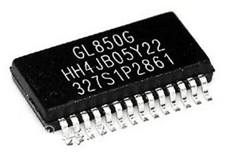
The GL850G USB 2.0 Hub Controller is a hub controller IC from Genesys Logic designed to expand one USB connection into multiple USB ports. It fully complies with the USB 2.0 specification and supports high-speed data transfer up to 480 Mbps.
The GL850G includes an embedded 8-bit RISC processor, built-in voltage regulators, power management support, status LED control, and EEPROM configuration for custom VID/PID settings. It also supports bus-powered and self-powered designs, giving system designers more flexibility. As a single TT hub controller, the GL850G offers a cost-effective solution for USB 2.0 hub designs while maintaining stable communication between the upstream host and downstream ports.
If you are interested in purchasing the GL850G, feel free to contact us for pricing and availability.
GL850G Main Features and Specifications
USB 2.0 Compliance and Data Transfer Support
The GL850G is fully compliant with USB Specification Revision 2.0, which means it can operate as a standard USB 2.0 hub controller. Its upstream port supports both high-speed and full-speed traffic, allowing it to communicate properly with the host system. The downstream ports support high-speed, full-speed, and low-speed USB devices, so different USB peripherals can connect through the same hub controller. It is also backward compatible with USB 1.1, making it suitable for older USB devices.
USB Communication Pipes
The GL850G includes one control pipe and one interrupt pipe for USB communication. The control pipe uses endpoint 0 with a 64-byte data payload and is mainly used for device setup, enumeration, and standard USB control requests. The interrupt pipe uses endpoint 1 with a 1-byte data payload and helps report hub status changes, such as device connection, disconnection, or port condition updates.
On-Chip 8-Bit Microprocessor
The GL850G has an on-chip 8-bit microprocessor that manages hub control functions internally. This processor uses a RISC-like architecture and a USB-optimized instruction set, allowing the chip to handle USB hub tasks efficiently. It operates at 6 MIPS at 12 MHz and includes 64-byte RAM and 4K mask ROM, which store and execute the basic control functions needed for hub operation.
Custom VID/PID and Port Configuration Support
The GL850G supports customized VID and PID settings through an external EEPROM or SMBUS. This allows manufacturers to assign their own vendor ID and product ID instead of using default settings. The downstream port configuration can also be programmed through EEPROM or SMBUS, giving designers more control over how many ports are enabled and how the hub appears to the host system.
Single Transaction Translator Architecture
The GL850G uses a Single Transaction Translator, or STT, architecture. This means one transaction translator is shared by all downstream ports when handling full-speed or low-speed devices connected to a high-speed USB 2.0 host. This design helps reduce cost and simplifies the hub controller, but performance may be more limited when several slower USB devices are active at the same time.
Integrated USB 2.0 Transceiver
The GL850G includes an integrated USB 2.0 transceiver, which handles the physical USB signaling between the hub controller, the host, and connected devices. This reduces the need for extra external components and helps simplify board-level design. The built-in transceiver supports stable signal communication for USB 2.0 hub operation.
EMI Reduction and ESD Recovery Support
The GL850G improves output drivers with slew-rate control to help reduce EMI, or electromagnetic interference. This is important because USB signal lines can generate noise if signal edges are too sharp or poorly controlled. The chip also includes internal power-fail detection for ESD recovery, helping the controller recover more safely after electrostatic discharge or power-related disturbances.
Low BOM Cost and Built-In Voltage Regulation
The GL850G is designed to reduce total board cost by integrating several required functions inside the chip. It includes a built-in 5V to 3.3V regulator, which reduces the need for an external 3.3V regulator in many designs. This helps lower BOM cost, saves PCB space, and makes the hub circuit easier to implement.
Built-In USB Pull-Up and Pull-Down Resistors
The GL850G includes a built-in upstream 1.5KΩ pull-up resistor and downstream 15KΩ pull-down resistors. These resistors are required for proper USB device detection and bus state control. By integrating them inside the chip, the GL850G reduces the number of external parts needed and helps simplify the USB hub circuit layout.
Clock and PLL Support
The GL850G has a built-in PLL that supports an external 12 MHz crystal or oscillator clock input. This clock source is important because USB communication requires accurate timing for reliable data transfer. The PLL helps generate the internal timing signals needed for USB 2.0 operation.
Low Power Support
The GL850G supports low-power operation, including selective suspend. Selective suspend allows the hub or connected ports to enter a lower-power state when they are not actively being used. It also supports LPM L1 with EEPROM, which helps improve power-saving behavior when configured properly. These features are useful for reducing power consumption in USB hub designs.
Smart Power Management
The GL850G supports smart power management for downstream ports. It can operate in both individual and gang power management modes, depending on the design and package type. Individual mode allows separate power control and over-current detection for each downstream port, while gang mode controls ports as a group. This gives designers flexibility in balancing cost, safety, and control.
Bus-Powered and Self-Powered Mode Support
The GL850G conforms to USB bus power requirements and supports automatic switching between self-powered and bus-powered modes. In bus-powered mode, the hub gets power from the upstream USB connection. In self-powered mode, the hub uses an external power source. Automatic switching helps the hub adapt to different power conditions without requiring complex external control.
Flexible Downstream Port Configuration
The number of downstream ports on the GL850G can be configured through SMBUS, EEPROM, or I/O pin settings depending on the design. This allows the same controller to support different hub layouts. It also supports compound-device configuration, where some downstream ports can be set as non-removable devices. This is useful when the hub controller is combined with internal USB functions on the same board.
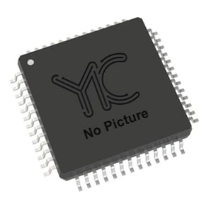
Available Package Options
The GL850G is available in several package options, including 28-pin QFN 5×5 mm, 28-pin SSOP 209 mil, and 24-pin QFN 4×4 mm. These package choices give designers flexibility based on PCB size, assembly process, and cost requirements. Smaller QFN packages are useful for compact layouts, while SSOP packages can be easier to handle in some manufacturing or prototyping conditions.
GL850G USB Hub Controller Functional Diagram
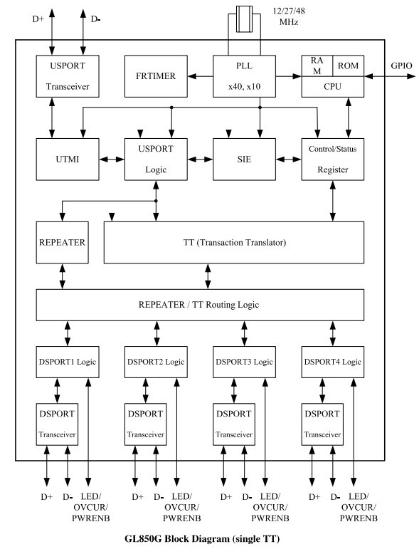
The GL850G functional block diagram shows how the USB hub controller manages communication between the host computer and multiple USB devices. At the top of the diagram, the upstream USB transceiver connects to the host through the D+ and D− lines. This section receives USB data from the computer and sends data back to the host. The built-in PLL uses an external 12/27/48 MHz clock source to generate stable internal timing signals required for USB communication.
Inside the controller, the CPU, RAM, ROM, SIE (Serial Interface Engine), and USB port logic work together to process USB packets, control hub functions, and manage data transfer. The CPU handles internal control operations, while the SIE processes USB protocol tasks such as packet decoding and device communication.
The Transaction Translator (TT) is one of the main blocks in the GL850G. It manages communication between high-speed USB 2.0 traffic and slower full-speed or low-speed USB devices connected to the downstream ports. Since the GL850G uses a single TT architecture, all downstream ports share the same translator logic.
At the bottom of the diagram, the repeater and downstream port logic distribute USB signals to multiple downstream USB ports. Each downstream port includes its own transceiver, power enable control, overcurrent detection, and LED status control signals for managing connected USB devices safely and reliably.
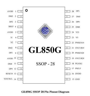
GL850G Pinout and Pin Functions
|
Pin
No. |
Pin
Name |
Pin
Function |
|
1 |
AVDD |
Analog power
supply input |
|
2 |
DM2 |
USB Port 2 D−
differential signal |
|
3 |
DP2 |
USB Port 2 D+
differential signal |
|
4 |
RREF |
Reference
resistor connection for internal circuit calibration |
|
5 |
AVDD |
Analog power
supply input |
|
6 |
X1 |
Crystal
oscillator or clock input |
|
7 |
X2 |
Crystal
oscillator output |
|
8 |
DM3 |
USB Port 3 D−
differential signal |
|
9 |
DP3 |
USB Port 3 D+
differential signal |
|
10 |
AVDD |
Analog power
supply input |
|
11 |
DM4 |
USB Port 4 D−
differential signal |
|
12 |
DP4 |
USB Port 4 D+
differential signal |
|
13 |
RESET# |
Active-low reset
input pin |
|
14 |
TEST/SCL |
Test mode pin or
SMBUS clock signal |
|
15 |
GND |
Ground
connection |
|
16 |
DVDD |
Digital power
supply input |
|
17 |
PSELF |
Self-powered
mode selection pin |
|
18 |
PGANG |
Gang power
management control pin |
|
19 |
OVCUR2# |
Overcurrent
detection input for Port 2 |
|
20 |
PWREN2# |
Power enable
output for Port 2 |
|
21 |
OVCUR1# |
Overcurrent
detection input for Port 1 |
|
22 |
PWREN1# |
Power enable
output for Port 1 |
|
23 |
V5 |
5V power input |
|
24 |
V33 |
Internal 3.3V
regulator output |
|
25 |
DM0 |
Upstream USB D−
differential signal |
|
26 |
DP0 |
Upstream USB D+
differential signal |
|
27 |
DM1 |
USB Port 1 D−
differential signal |
|
28 |
DP1 |
USB Port 1 D+
differential signal |
GL850G Typical Application Design
The GL850G typical application circuit shows how the hub controller is connected to the upstream USB port, downstream USB ports, clock source, power supply, and protection components. The GL850G acts as the main control IC that receives USB data from the host device through the upstream D+ and D− lines, then distributes the USB connection to multiple downstream USB ports.
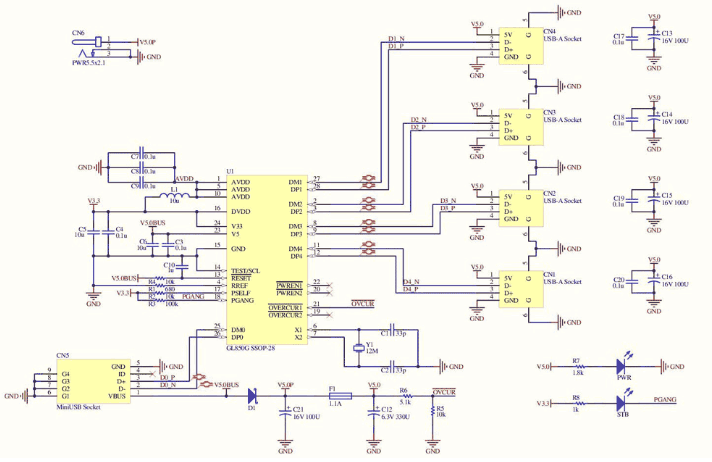
At the lower-left side of the circuit, the Mini USB connector is used as the upstream USB connection to the computer or host system. The upstream USB data lines connect directly to the GL850G upstream pins. A diode and fuse are added to help protect the circuit from reverse current and overcurrent conditions.
The crystal oscillator connected to the X1 and X2 pins provides the 12 MHz clock signal required for USB timing operation. Capacitors connected around the power pins help filter noise and stabilize the power supply for reliable USB communication.
On the right side of the circuit, the downstream USB ports are connected to the GL850G through separate D+ and D− signal lines. Each USB port also includes decoupling capacitors for power filtering. The PWREN and OVCUR pins are used for USB port power control and overcurrent detection, helping protect connected USB devices.
To use the GL850G, typically connect the upstream USB port, add a 12 MHz crystal, provide stable 5V power input, connect the downstream USB ports, and configure the power management pins properly. This allows the GL850G to function as a complete USB 2.0 hub controller with multiple downstream USB ports.
GL850G vs Other USB Hub Controllers
|
Feature |
GL850G |
GL852 |
FE1.1s |
USB
3.0 Hub Controllers |
|
USB Standard |
USB 2.0 |
USB 2.0 |
USB 2.0 |
USB 3.0 / USB
3.2 |
|
Maximum Speed |
480 Mbps |
480 Mbps |
480 Mbps |
5 Gbps or higher |
|
Transaction
Translator |
Single TT |
Multiple TT |
Single TT |
Multiple TT |
|
Performance With
Multiple USB Devices |
Moderate |
Better handling
of mixed-speed devices |
Basic
performance |
High-performance
multi-device support |
|
Cost |
Low |
Slightly higher
than GL850G |
Very low |
Higher |
|
Internal
Processor |
Built-in 8-bit
MCU |
Built-in MCU |
Simpler internal
architecture |
More advanced
controller architecture |
|
Power Management |
Individual and
gang mode support |
Advanced power
management |
Basic power
control |
Advanced smart
power management |
|
EEPROM / SMBUS
Support |
Yes |
Yes |
Limited |
Yes |
|
Best For |
Cost-effective
USB hubs |
Better USB 2.0
hub performance |
Simple low-cost
USB hubs |
High-speed
modern USB hubs |
|
Power
Consumption |
Low |
Low |
Very low |
Higher than USB
2.0 hubs |
|
Design
Complexity |
Moderate |
Moderate |
Simple |
More complex PCB
design |
|
Typical
Limitation |
Shared TT
bandwidth |
Higher cost |
Fewer advanced
features |
Higher cost and
power requirement |
Best Applications of GL850G
• USB 2.0 Hub Devices - Commonly used in multi-port USB hubs to expand one USB connection into several USB ports.
• Laptop Docking Stations - Helps add extra USB connectivity for keyboards, mice, flash drives, and printers.
• Embedded Systems - Used in embedded boards and industrial controllers that require multiple USB device connections.
• Industrial USB Expansion - Suitable for industrial equipment that needs stable USB communication with multiple peripherals.
• DIY USB Hub Projects - Popular among electronics hobbyists because of its low cost and relatively simple circuit design.
• Single Board Computer (SBC) Projects - Often integrated into Raspberry Pi and Linux-based systems for additional USB ports.
• USB Interface Modules - Used in systems that combine multiple USB devices into one compact board design.
• POS and Kiosk Systems - Helps connect barcode scanners, receipt printers, card readers, and other USB peripherals.
• Computer Monitor USB Hubs - Integrated inside monitors that provide built-in USB expansion ports.
• Low-Cost Consumer Electronics - Used in affordable USB accessories where USB 2.0 speed is sufficient for normal peripherals.
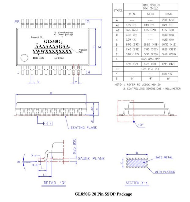
Mechanical Dimensions of GL850G
Manufacturer
Genesys Logic, the manufacturer of the GL850G, is a semiconductor company specializing in USB hub controllers, storage controllers, and interface IC solutions. The company supports large-scale IC manufacturing through advanced semiconductor design, packaging, testing, and quality control processes to ensure stable product performance and long-term reliability. Genesys Logic focuses on low-cost, highly integrated controller solutions that simplify PCB design and reduce BOM cost for manufacturers.
Frequently Asked Questions [FAQ]
1. Why does the GL850G use a Single Transaction Translator instead of Multiple Transaction Translators?
The GL850G uses a Single Transaction Translator (STT) mainly to reduce overall chip cost and simplify the hub architecture. In this design, all downstream full-speed and low-speed USB devices share the same transaction translator logic. This works well for normal USB peripherals like keyboards, mice, printers, and flash drives. However, if several slower USB devices transfer data heavily at the same time, bandwidth sharing may slightly reduce performance compared to multi-TT hub controllers.
2. How does the built-in 5V to 3.3V regulator help simplify USB hub design?
The integrated 5V to 3.3V regulator removes the need for a separate external regulator in many hub circuits. This helps reduce PCB space, lowers BOM cost, and simplifies power design. It also makes the overall USB hub circuit smaller and easier to manufacture.
3. Why is the 12 MHz crystal important in the GL850G circuit?
The 12 MHz crystal provides the reference clock needed for accurate USB timing. The built-in PLL multiplies this clock internally to generate stable timing signals for USB communication. Without accurate clock timing, USB data transfer can become unstable or fail completely.
4. What is the advantage of supporting both bus-powered and self-powered modes?
Supporting both modes gives designers more flexibility. Bus-powered mode allows the USB hub to operate directly from the host USB port, which is useful for compact low-power hubs. Self-powered mode uses an external power supply, allowing the hub to support higher-current USB devices more reliably.
5. How does the GL850G improve EMI performance in USB hub designs?
The GL850G includes slew-rate control in its output drivers to reduce sharp signal transitions on USB data lines. This helps lower electromagnetic interference (EMI), which improves signal stability and reduces the chance of communication problems caused by electrical noise.
6. Why are overcurrent detection and power enable pins important in USB hubs?
The OVCUR and PWREN pins help protect both the hub and connected USB devices. If a connected device draws too much current, the hub can detect the fault and disable power to the affected port. This improves safety and helps prevent hardware damage.
7. How does EEPROM support improve the flexibility of the GL850G?
EEPROM support allows manufacturers to customize VID, PID, downstream port settings, and power management behavior. This helps companies create branded USB hubs and configure the controller for different hardware designs without changing the main chip.
Σχετικό άρθρο
-
![Οδηγός Ηλεκτρονικών εξαρτημάτων Key Smartwatch]() May 19 2026Οδηγός Ηλεκτρονικών εξαρτημάτων Key Smartwatch
May 19 2026Οδηγός Ηλεκτρονικών εξαρτημάτων Key SmartwatchΜέσα σε ένα smartwatch υπάρχει ένα συμπαγές σύστημα ηλεκτρονικών εξαρτημάτων που συνε...

Σχετικά προϊόντα
TLJT107M006R0800
CAP TANT 100UF 20% 6.3V 1411
EP20K200EFC484-2X
IC FPGA 376 I/O 484FBGA

SA53488434
IGBT Modules

V300C48H150AN
IGBT Modules
CXD2411R
SONY QFP
AM6968NE-T1-PF
AM6968NE-T1-PF A

LTC1326IMS8
LTC1326IMS8 LINEAR

AT27LV520-70SI
AT27LV520-70SI ATMEL

S3CA460S01-YX80
S3CA460S01-YX80 SAMSUNG

AD8560ACP-REEL7
IC BUFFER AMP 5CH 16V 16-LFCSP

MAX4447ESE
MAX SOP-16

UPD78F1828AGAA-GAM-E2-G
RENESAS LQFP48
LTC3411EDD#TR
LINEAR QFN